New equipment coming this year to Cornell University in Ithaca, New York will give NORDTECH members access to exceptional capabilities for research, product development and prototyping in the four Technology Focus Areas: Quantum Technology, AI Hardware, Secure Edge Computing, and Commercial Leap Ahead.
The new equipment, hosted at the Cornell NanoScale Science and Technology Facility (CNF), vastly expands the lab-to-fab capabilities available in New York state for microelectronic researchers, startups and other innovators. Funding for the new equipment, which represents the largest capital expansion of CNF since its establishment in 1977, was provided by the U.S. Department of Defense Microelectronics Commons program through NORDTECH. NORDTECH’s five founding members who comprise the leadership team / governance committee of the hub include: NY CREATES, the University at Albany College of Nanotechnology, Science, and Engineering (CNSE), Cornell University, Rensselaer Polytechnic Institute (RPI), and IBM.
Contact CNF at userprogram (at) cnf.cornell.edu to initiate a project. In most cases, projects can be reviewed, screened and approved within 2 weeks of initial contact. Additional information for prospective users is available at Starting a New Project at the CNF.
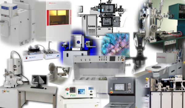
Several new tools are on schedule to arrive by year end:
- The new Keyence VHX7100 Digital Inspection Microscope (available now) offers 200 mm capability, 4K ultra-high accuracy, and 12-megapixel video resolution with screen magnifications to 6000x. It performs a wide variety of 2D and 3D measurements, including 3D renderings of topography. This tool enables researchers to quickly identify issues that arise during process – a critical inspection tool for projects across multiple focus areas including Quantum Technology.
- The Maskless Photolithography System (Heidelberg MLA150) provides rapid prototyping of pattern design and offers in situ electronic mapping and electrical connection for 2D materials with nonstandard shapes. Researchers can rapidly iterate quantum device configurations on complex qubit designs for composite Josephson supercomputing circuits without the need for a new photomask. 200 mm capability.
- The Zeiss Gemini 560 Scanning Electron Microscope offers superior imaging at extremely low beam energies < 100 eV. Researchers can inspect an entire 200 mm wafer without rotation.
- A Temporary Bonding/Debonding System (Osiris International Affix 20m/Defix 20m) provides temporary bonding and debonding of wafer assemblies to create mechanical support for devices. The system enables backside processing for 3D integration, making it critical for projects in multiple focus areas, especially Quantum Technology.
- The Polyimide Cure Oven (Yield Engineering PB8) is a laminar flow high-temperature vacuum cure oven (up to 450 °C). This critical packaging technology infrastructure enables curing of polyimide, epoxy, and wafer-to-wafer bonding annealing, in particular for quantum packaged integrated parts.
- A new system for Chemical Mechanical Polishing for 200 mm wafers extends CNF’s current chemical mechanical polishing (CMP) and post-CMP cleaning capabilities to 200 mm wafers. Users can process multiple substrate sizes, including pieces, 100 mm, 150 mm and 200 mm.
CNF maintains a comprehensive set of advanced nanofabrication tools for lithography, etching, deposition, film growth, characterization and more, supported by technical staff with a broad range of expertise. Projects span the breadth of nanotechnology, with extensive resources in electronics, materials science, biology, chemistry and physics.
Coming in 2025: a 200 mm-capable Atomic Layer Deposition system (Oxford PlasmaPro ASP) that can deposit superconducting materials and nitride materials; a UHV Evaporator and Oxidation System that can deposit ultra-clean films, including quantum qubit PVD thin materials, and is equipped with oxidation capabilities to directly form Josephson junctions in situ; a versatile UHV Sputtering System with particular application for quantum projects, including Josephson junction deposition, hot sputtering for refractory metal superconductor films (Ta, Nb), and deposition of nitride films for magnetic field-compatible superinductance; a Diamond CVD System; a Wafer Back Grinder with 200 mm capability for producing ultra-thin wafers used in high density packaging (e.g. chiplets) and QST heterointegration; a next-generation Plasma Dicing/Singulation tool; a Deep Oxide/Diamond Etcher (ICP RIE); a high-temperature vapor XeF2 etch system; and a 200 mm-capable Electroplating System that supports indium and Sn/Ag/Cu plating.
CNF is an open user facility and a member of the National Nanotechnology Coordinated Infrastructure (NNCI) supported by the National Science Foundation (NSF).